The Future of Electron Beam Curing
Electron beam curing has a number of significant advantages in comparison to wet paints and powder coating.

Or read the article in our August Digital Edition.
 The first experiments with electron beams date from as early as 1920 in the United States, but the first attempts to cure varnishes with electron beam curing (EBC) were only made in 1960. The essence of EBC is that an electron bundle induces crosslinking in a coating that has been applied, which actually involves radical polymerization as we know it from organic chemistry. This crosslinking is only possible if the varnish contains double bonds, for example in the form of ethylene, propylene, vinyl or acrylate groups. The last of these are particularly popular for their combination of properties.
Electrons Accelerated in Electrical Field
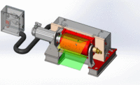
The electrons are generated by conducting an electrical current through a tungsten filament and then accelerated in an electrical field that is applied. This is done in a vacuum, which is closed off by a titanium foil window that is permeable to electrons. The technique primarily lends itself to flat products, although the range of the electrons is adequate to be able to handle a certain profile height.
The product with the applied coating or ink is then guided underneath the titanium window for exposure to the beam. An inert atmosphere is necessary because the presence of oxygen causes a number of undesired reactive bonds in the coating. Nitrogen with at least 99.98 percent purity is usually used for this, or an oxygen content of less than 200 ppm.
Dose and Energy Density
There are two primary variables with EBC: the dose and the energy density of the electrons. The dose, which is the quantity of electrons that are fired at the coating, depends on the temperature of the filament, or the current intensity and/or voltage. The dose determines the speed of crosslinking, or the degree of crosslinking that can be obtained in combination with a certain feed rate.
The high-voltage electrical field that is applied determines the energy of the electrons and therefore their penetration depth into the ink or coating to be cured. For coatings and inks, a voltage between 70 kV and 300 kV is generally adequate. This gives a penetration depth of about 15 µm and 500 µm respectively, although this also depends on the density of the coating material. It is important to tune this properly, because with too low a voltage the coating does not cure to the full depth, and with too high a voltage the substrate may be unnecessarily influenced. Aside from unnecessary energy consumption, this can lead to discoloration.
Low Energy Consumption and No Waste Products
EBC has a number of significant advantages in comparison to wet paints and powder coating. First of all, there are absolutely no organic or other solvents, making it environmentally friendly with no CO2 emissions. To be able to use the materials for coating processes, only low-molecular-weight polyethylene glycols (PEGs), propylene glycol acrylates (PGAs) or other multifunctional compounds are added as ‘solvents’.
Another advantage is the low energy consumption. If issues such as cooling are included in the calculations, the differences are great. The CO2 emissions are also many times lower.
Furthermore, the crosslinking reactions with EBC are fast and complete. Other advantages include scratch resistance, chemical resistance and color fastness.
EBC Conversion to Overcome Initial Barriers
A major barrier still to conversion to EBC is the initial cost involved. This is due to the vacuum chamber that is needed, the high voltage power supply to generate the voltage, and the need to create an inert atmosphere. Because of the unsurpassed characteristics of the resulting coating and the environmentally friendly aspects, issues such as energy consumption and avoiding waste water and waste gases will become increasingly important in the future. Things are happening, and it is one of RadTech Europe's priorities to make the industry aware of the quality and value EBC can bring. One of the platforms serving this purpose is RadTech Europe's bi-annual conference and exhibition, which is taking place this year on the 15 - 17th of October in Basel, Switzerland.
About RadTech
RadTech Europe (RTE), founded in 1988 in Basel (Switzerland) and headquartered in The Hague (The Netherlands), is the European industry association that promotes the development, use and benefits of UV/EB curing technology for inks, coatings and adhesives. For more information, visit www.radtech-europe.com.
Looking for a reprint of this article?
From high-res PDFs to custom plaques, order your copy today!


